 Machine learning has great potential, but it is not a silver bullet. It cannot provide generalized solutions, in which one feeds any data to an algorithm and expects meaningful results. For it to be effective, it needs a good data set that can be used for training and the right algorithm. Accuracy of the results should be evaluated and adjustments made to optimize results. During this process, one has to adopt newer, more accurate algorithms or enhanced types of existing algorithms. In most, if not all cases, it takes time before a good solution is obtained, in particular if the data set is messy.
Machine Learning Is Not A Single Step Process
Hype led to a gross over-simplification of machine learning. The focus is on any results,  not on what it takes to attain good results. For instance, many give face recognition as an example of the success of machine learning. They forget to mention that the work on face recognition started more than 26 years ago, before 1989, by Kohonen, Kirby and Sirovich. Even after the advent of powerful computers in the early 2000’s, it took a while before it matured. Newer algorithms developed in 2006, are 10 times more accurate than the face recognition algorithms of 2002 and 100 times more accurate than those of 1995.
Semiconductor: Great Machine Learning Success
The Semiconductor Industry have been very successful in adopting machine learning. Solutions were contemplated without hype or fanfare. It has been a solid approach based on defining the problem, understanding the data, selecting the right algorithm, implementing a solution and adapting it whenever there are changes. Machine learning algorithms can be very demanding from a computational point of view. A pragmatic approach is to is to optimize solutions and tailor them to the available computing power. As the structure of semiconductor devices changed over the last 20 years, new solutions were adopted based on new data and new algorithms.
Why Machine Learning Is Important For The Semiconductor Industry
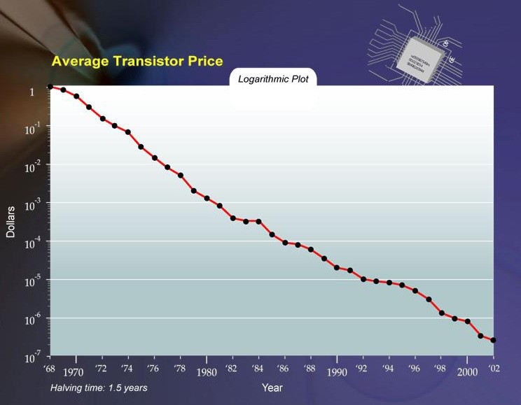
Automatic defect detection in wafers based on machine learning is a critical component of the wafer manufacturing process. The objective is to increase the yield which is defined as the percentage of chips in a finished wafer that pass all tests and function properly. Higher yield means lower manufacturing costs, higher profitability and cheaper devices. Increasing the yield is the main reason that drives the prices of semiconductor devices down and makes computers, cell phones and other products affordable. A measure of machine learning success is the unprecedented drop in the prices of semiconductor devices, as shown below.

Techniques Used For Machine Learning
Techniques used for machine learning in The Semiconductor Industry have changed as semiconductor devices changed. Some of those techniques are:
- Capture bright-field images of patterned wafers and look for defects by comparing die images (die-to-die comparison).
- Dark-field tools that measure defects and particles on patterned wafers.
- Bright field tools became more sensitive with higher resolution microscope objectives, and are used in cell-to-cell comparisons for array regions of the die, and in die-to-die comparisons for logic regions.
- Electron beam wafer inspection systems detect very small defects which are difficult to detect with optical systems.
- Broadband plasma defect inspection systems.
- Defect detection in patterned wafers using Scanning Electron Microscope (SEM) images.
The Lessons Learned
- The hype needs to be tempered. Machine learning does not provide an ultimate solution. It is a compromise of several elements: complexity of the algorithm, quality of input data, computing power available, and accuracy.
- Define the problem, understand data, find an accurate solution and verify.
- If an algorithm requires more computing power than current computers can provide, make adjustments to the algorithm, without sacrificing accuracy. For instance, if an algorithm requires a convolving window, reduce the size of the window, and make sure the reduction does not render the solution useless.
- There is nothing called an absolute or final solution. As devices change, adapt the technology or implement a new solution.
- At each step quantify accuracy and perform statistical analysis.
- Anticipate changes in devices, input data and work on a new solution.
- Assign an integrated team to work on defect detection, instead of creating a data scientist position that requires an unrealistic skill set.
